| CPC H01S 5/1003 (2013.01) [H01S 5/026 (2013.01); H01S 5/04256 (2019.08)] | 18 Claims |

|
1. A semiconductor light emitting element that outputs laser light, the semiconductor light emitting element comprising:
a first conductive type first clad layer;
an active layer arranged on the first clad layer;
a second conductive type second clad layer arranged on the active layer;
an upper electrode electrically connected to the second clad layer; and
a lower electrode electrically connected to the first clad layer, wherein
a portion where the first clad layer, the active layer, and the second clad layer are layered constitutes an optical waveguide,
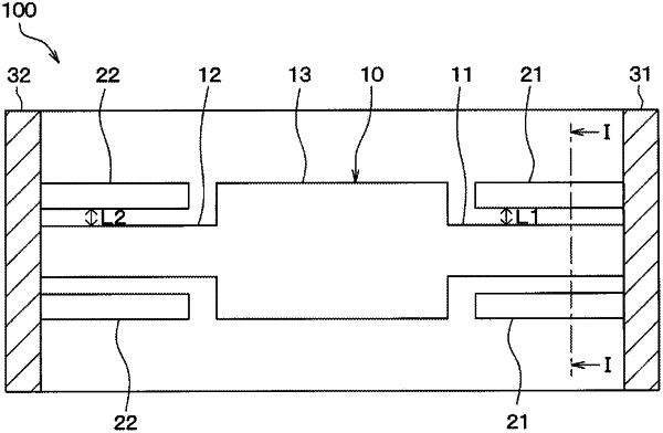
the optical waveguide includes a first waveguide and a second waveguide respectively having widths capable of propagating light in a second-order mode or higher, and a multimode optical interference waveguide arranged between the first and second waveguides and having a width wider than the first and the second waveguides,
a first optical loss layer is provided to face the first waveguide in an active-layer crossing direction for causing a loss of light that is propagating in the first waveguide in the second-order mode or higher, and a second optical loss layer is provided to face the second waveguide in an active-layer crossing direction for causing a loss of light that is propagating in the second waveguide in the second-order mode or higher, the active-layer crossing direction being a direction orthogonal to a surface of the active layer,
the first waveguide is not in direct physical contact with the first optical loss layer, and
the second waveguide is not in direct physical in contact with the second optical loss layer.
|