| CPC H01L 33/62 (2013.01) [H01L 25/0753 (2013.01); H01L 33/0093 (2020.05); H01L 33/382 (2013.01); H01L 2933/0016 (2013.01); H01L 2933/0066 (2013.01)] | 22 Claims |

|
1. A method for making a display panel, comprising:
providing a substrate;
preparing a driving circuit layer on one side of the substrate; wherein driving circuit layer preparing comprises a binding layer, a display base, and an array circuit layer which are stacked, and the binding layer is located on between the display base and the substrate; wherein the preparing a driving circuit layer on one side of the substrate comprises:
forming the binding layer on the surface of the substrate; and
depositing an insulating layer on the substrate; wherein the insulating layer is non-free-standing and deposited by a thick film process or by a coating process, the insulating layer is oxide insulating layer or nitride insulating layer, the thickness of the insulating layer is less than the thickness of a hard substrate or the thickness of a flexible layer, and the overall thickness of the display panel is reduced;
forming a first through hole in the insulating layer;
depositing a first metal layer on the surface of the insulating layer away from the substrate; wherein the first metal layer is partially arranged in the first through hole and electrically connected to the binding layer;
patterning the first metal layer to form a connecting portion electrically connected to the binding layer;
forming a semiconductor layer on the side of the insulating layer away from the binding layer;
doping the semiconductor layer to form a channel, a source, and a drain;
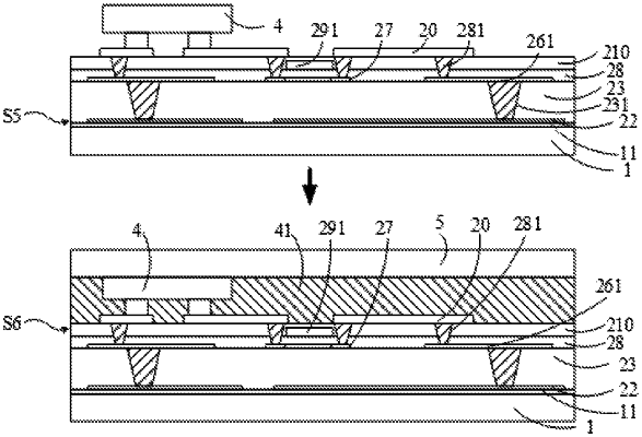
disposing a plurality of light emitting units on one side of the array circuit layer away from the substrate; wherein the light emitting units are electrically connected to the array circuit layer;
disposing a cover substrate on one side of the plurality of light emitting units away from the substrate; wherein, the cover substrate is free-standing;
removing the substrate to expose the binding layer, wherein removing the substrate to expose the binding layer comprises: keeping the plurality of the light emitting units, the driving circuit layer, the insulating layer and the binding layer being subsequently arranged on the cover substrate, wherein the plurality of the light emitting units, the driving circuit layer, the insulating layer and the binding layer are supported by the cover substrate;
binding an external control unit on the binding layer.
|