| CPC H01L 33/0093 (2020.05) [H01L 33/0095 (2013.01); H01L 33/62 (2013.01); H01L 25/0753 (2013.01); H01L 25/167 (2013.01); H01L 33/0075 (2013.01); H01L 33/32 (2013.01); H01L 2933/0066 (2013.01)] | 2 Claims |

|
1. A method for manufacturing a semiconductor device, comprising:
forming a plurality of light-emitting elements on a first substrate;
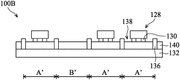
forming a first pattern array on a second substrate, wherein the first pattern array comprises an adhesive layer, the adhesive layer is formed on a first portion of the second substrate and not formed on a second portion of the second substrate;
transferring the plurality of light-emitting elements from the first substrate to the second substrate;
forming the first pattern array on a third substrate;
transferring the plurality of light-emitting elements from the second substrate to the third substrate;
forming a second pattern array on a fourth substrate; and
transferring the plurality of light-emitting elements from the third substrate to the fourth substrate,
wherein the adhesive layer on the first portion is surrounded by a plurality of spacer layers on the third substrate, and the plurality of light-emitting elements are transferred from the first portion of the third substrate rather than the second portion of the third substrate to the fourth substrate,
wherein a pitch between the plurality of light-emitting elements on the first substrate is different than a pitch of the first pattern array.
|