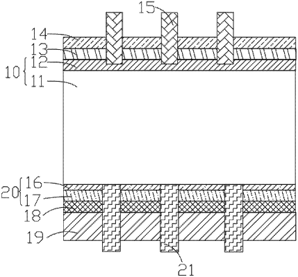
| CPC H01L 31/02168 (2013.01) [H01L 31/02167 (2013.01); H01L 31/1868 (2013.01)] | 20 Claims |

|
1. A photovoltaic cell, comprising:
a silicon substrate;
a first passivation layer disposed on a front surface of the silicon substrate; and
a second passivation layer, at least one silicon oxynitride layer, and at least one silicon nitride layer that are disposed on a rear surface of the silicon substrate in a direction away from the silicon substrate;
wherein the second passivation layer comprises a first silicon oxide layer and at least one aluminum oxide layer, a ratio of a number of oxide atoms to a number of aluminum atoms in the at least one aluminum oxide layer is greater than 0.8 and less than 1.6, and a thickness of the at least one aluminum oxide layer is in a range of 4 nm to 20 nm; wherein a number of silicon atoms is greater than a number of oxygen atoms in the at least one silicon oxynitride layer and the number of oxygen atoms is greater than a number of nitrogen atoms in the at least one silicon oxynitride layer, and a thickness of the at least one silicon oxynitride layer is in a range of 1 nm to 30 nm; and wherein a ratio of a number of silicon atoms to a number of nitrogen atoms in the at least one silicon nitride layer is greater than 1 and less than 4, and a thickness of the at least one silicon nitride layer is in a range of 50 nm to 100 nm.
|