| CPC H01L 29/872 (2013.01) [H01L 29/0619 (2013.01); H01L 29/868 (2013.01)] | 11 Claims |

|
1. A wide-band gap semiconductor device, comprising:
a substrate;
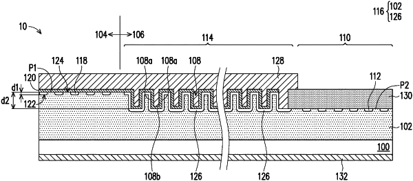
an epitaxial layer disposed on the substrate, wherein the epitaxial layer includes a first plane, a second plane around the first plane, a plurality of trenches between the first plane and the second plane, and the second plane is closer to the substrate than the first plane;
an array of merged PN junction Schottky (MPS) diode, formed in the first plane of the epitaxial layer; and
an edge termination area surrounding the array of MPS diode, wherein the edge termination area comprises:
a floating ring region having a plurality of floating rings formed in the second plane of the epitaxial layer; and
a transition region between the floating ring region and the array of MPS diode, wherein the transition region comprises a PIN diode formed on the plurality of trenches and on the epitaxial layer between the trenches,
wherein the array of MPS diode comprises:
a plurality of first p+ doping regions in the epitaxial layer to form a PN junction between the epitaxial layer and each of the first p+ doping regions; and
a Schottky metal layer disposed on the epitaxial layer to form a plurality of Schottky diodes with the epitaxial layer among the first p+ doping regions.
|