| CPC H01L 29/7869 (2013.01) [H01L 29/4966 (2013.01); H01L 29/517 (2013.01)] | 18 Claims |

|
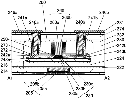
1. A semiconductor device comprising:
a first insulator;
a first oxide over the first insulator;
a second oxide over and in contact with the first oxide;
a first conductor over the second oxide;
a second conductor over the second oxide;
a second insulator covering the first oxide, the second oxide, the first conductor, and the second conductor;
a third insulator over the second insulator;
a third oxide over the second oxide, the third oxide being provided in an opening of the third insulator;
a fourth insulator over the third oxide; and
a third conductor over the third insulator,
wherein the third oxide is in contact with a top surface of the second oxide, a first side surface of the first conductor and a first side surface of the second conductor,
wherein the third oxide is in contact with a side surface of the third insulator in the opening,
wherein the second oxide comprises In, an element M, and Zn, where the element M is Al, Ga, Y, or Sn,
wherein the second insulator is in contact with a top surface of the first conductor, a top surface of the second conductor, a second side surface of the first conductor, a second side surface of the second conductor, a side surface of the second oxide, and a side surface of the first oxide, and
wherein the third oxide comprises aluminum.
|