| CPC H01L 29/7869 (2013.01) [H01L 29/66969 (2013.01); H10B 61/22 (2023.02); H10B 63/30 (2023.02)] | 20 Claims |

|
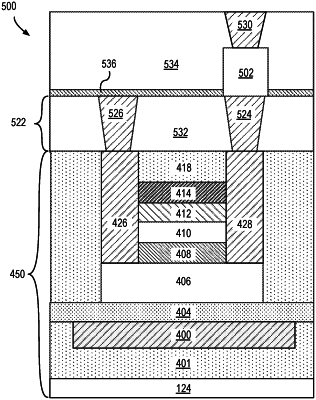
1. A thin film transistor (TFT) structure, comprising:
a gate electrode;
a gate dielectric layer on the gate electrode;
a channel layer on the gate dielectric layer, wherein the channel layer comprises a semiconductor material with a first polarity and comprising a first metal and oxygen;
a multi-layer material stack on the channel layer, opposite the gate dielectric layer;
a dielectric material over the multi-layer material stack and beyond a sidewall of the channel layer; and
source and drain contacts through the dielectric material, and in contact with the channel layer, wherein the multi-layer material stack comprises:
a first layer in contact with the channel layer,
wherein the first layer comprises a second metal absent from the channel layer, and wherein the first layer has a second polarity, complementary to the first polarity; and
a second layer in contact with the first layer, wherein the second layer and the dielectric material have different compositions.
|