US 11,955,557 B2
Semiconductor device and manufacturing method thereof
Shunpei Yamazaki, Tokyo (JP); and Jun Koyama, Kanagawa (JP)
Assigned to Semiconductor Energy Laboratory Co., Ltd., Atsugi (JP)
Filed by Semiconductor Energy Laboratory Co., Ltd., Atsugi (JP)
Filed on Aug. 31, 2022, as Appl. No. 17/899,654.
Application 17/899,654 is a continuation of application No. 17/172,261, filed on Feb. 10, 2021, granted, now 11,456,385.
Application 17/172,261 is a continuation of application No. 16/720,151, filed on Dec. 19, 2019, granted, now 10,944,010, issued on Mar. 9, 2021.
Application 16/720,151 is a continuation of application No. 15/919,437, filed on Mar. 13, 2018, granted, now 10,516,055, issued on Dec. 24, 2019.
Application 15/919,437 is a continuation of application No. 14/974,627, filed on Dec. 18, 2015, granted, now 10,056,494, issued on Aug. 21, 2018.
Application 14/974,627 is a continuation of application No. 14/287,320, filed on May 27, 2014, granted, now 9,219,162, issued on Dec. 22, 2015.
Application 14/287,320 is a continuation of application No. 13/770,022, filed on Feb. 19, 2013, granted, now 8,742,544, issued on Jun. 3, 2014.
Application 13/770,022 is a continuation of application No. 12/945,243, filed on Nov. 12, 2010, granted, now 8,410,002, issued on Apr. 2, 2013.
Claims priority of application No. 2009-260368 (JP), filed on Nov. 13, 2009.
Prior Publication US 2022/0416087 A1, Dec. 29, 2022
Int. Cl. H01L 29/786 (2006.01); H01L 29/04 (2006.01); H01L 29/24 (2006.01); H01L 29/45 (2006.01); H01L 29/66 (2006.01)
CPC H01L 29/78618 (2013.01) [H01L 29/045 (2013.01); H01L 29/24 (2013.01); H01L 29/45 (2013.01); H01L 29/66757 (2013.01); H01L 29/66969 (2013.01); H01L 29/7869 (2013.01); H01L 29/78696 (2013.01)] 8 Claims
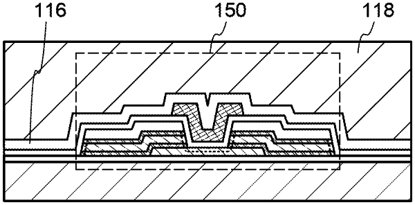
OG exemplary drawing
 
1. A semiconductor device comprising:
a first insulating layer;
an oxide semiconductor layer over the first insulating layer;
a gate electrode over the oxide semiconductor layer;
a first electrode in contact with an upper surface of the oxide semiconductor layer;
a second insulating layer in contact with the first electrode; and
a third insulating layer over the first electrode,
wherein the oxide semiconductor layer comprises indium, gallium, and zinc,
wherein the second insulating layer, the first electrode, and the oxide semiconductor layer overlap with one another in a direction perpendicular to the upper surface of the oxide semiconductor layer,
wherein the third insulating layer is in contact with the gate electrode, an upper surface and a side surface of the second insulating layer, a side surface of the first electrode, an upper surface of the first insulating layer, and the upper surface of the oxide semiconductor layer, and
wherein each of an end portion of the second insulating layer and an end portion of the first electrode has a tapered shape.