| CPC H01L 29/78618 (2013.01) [H01L 21/02236 (2013.01); H01L 21/02532 (2013.01); H01L 21/02603 (2013.01); H01L 29/0673 (2013.01); H01L 29/42392 (2013.01); H01L 29/66545 (2013.01); H01L 29/66636 (2013.01); H01L 29/66742 (2013.01); H01L 29/78696 (2013.01)] | 20 Claims |

|
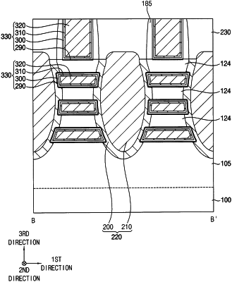
1. A method of manufacturing a semiconductor device, the method comprising:
forming a fin structure, the fin structure including sacrificial lines and semiconductor lines that are alternately and repeatedly stacked in a vertical direction, the vertical direction perpendicular to an upper surface of a substrate;
forming a dummy gate structure on the substrate covering a portion of the fin structure;
removing a portion of the fin structure at each of first and second sides of the dummy gate structure to form a first opening, the first side opposite the second side;
forming a source/drain layer in the first opening;
forming an insulating interlayer on the substrate covering the dummy gate structure and the source/drain layer;
removing the dummy gate structure and the sacrificial lines to form second and third openings, respectively, the third opening exposing a portion of a sidewall of the source/drain layer;
oxidizing the exposed portion of the sidewall of the source/drain layer to form an oxide layer;
removing the oxide layer to form a fourth opening, the fourth opening having an enlarged width greater than a width of the third opening, the width of the third opening and the fourth opening in a horizontal direction that is parallel to the upper surface of the substrate; and
forming a gate structure in the second and fourth openings.
|