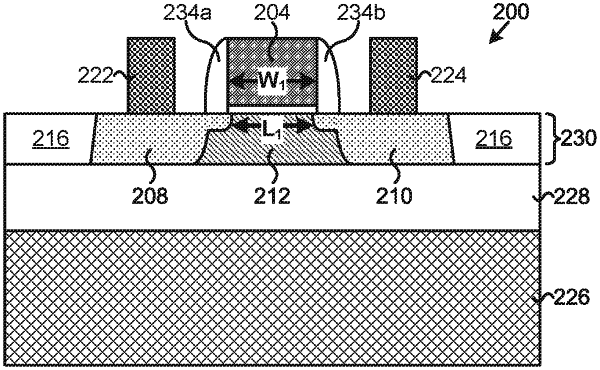
| CPC H01L 29/78609 (2013.01) [H01L 21/76202 (2013.01); H01L 21/76224 (2013.01); H01L 27/1203 (2013.01); H01L 29/402 (2013.01)] | 19 Claims |

|
1. A field effect transistor (FET) comprising:
an active region including a source region, a drain region, and a channel region, said channel region under a gate and situated between said source region and said drain region;
a field region next to said active region, said channel region having an interface with said field region;
said gate having a wide outer gate segment proximate to said interface and a narrow inner gate segment distant from said interface;
said wide outer gate segment producing an outer channel length greater than an inner channel length produced from said narrow inner gate segment, thereby reducing a leakage current of said FET during an OFF state.
|