| CPC H01L 29/785 (2013.01) [H01L 21/02694 (2013.01); H01L 21/324 (2013.01); H01L 21/76829 (2013.01); H01L 21/823814 (2013.01); H01L 21/823864 (2013.01); H01L 29/6681 (2013.01)] | 20 Claims |

|
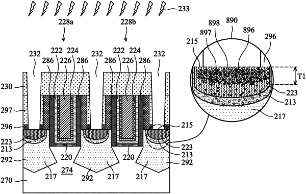
11. A method of forming a semiconductor device, the method comprising:
forming a doped active region on a substrate, the doped active region including a first region having a first germanium concentration and a second region having a second germanium concentration, the first germanium concentration being greater than the second germanium concentration, the first region being over the second region;
forming a dielectric layer over the doped active region;
forming an opening through the dielectric layer to expose an exposed region of the first region of the doped active region;
implanting a first dopant into the exposed region, wherein the first dopant has a larger molecule size than a molecule of a material of the doped active region;
after implanting the first dopant, implanting at least a second dopant comprising a p-type dopant or an n-type dopant into the doped active region containing the first dopant;
performing a plurality of anneal processes;
after performing the plurality of anneal processes, forming a silicide region at an upper surface of the exposed region; and
forming a conductive feature in the opening to the silicide region.
|