| CPC H01L 29/7833 (2013.01) [H01L 21/823807 (2013.01); H01L 21/823814 (2013.01); H01L 21/823828 (2013.01); H01L 21/823864 (2013.01); H01L 21/823871 (2013.01); H01L 29/04 (2013.01); H01L 29/0649 (2013.01); H01L 29/165 (2013.01); H01L 29/6653 (2013.01); H01L 29/66545 (2013.01); H01L 29/6656 (2013.01); H01L 29/6659 (2013.01); H01L 29/66628 (2013.01); H01L 29/66636 (2013.01); H01L 29/7834 (2013.01); H01L 29/7848 (2013.01)] | 20 Claims |

|
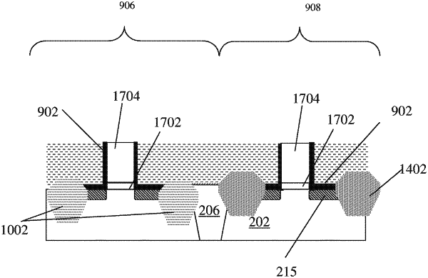
1. An integrated circuit device comprising:
a first gate stack and a second gate stack disposed over a substrate;
a first silicon carbonitride (SiCN) spacer liner, a second SiCN spacer liner, a third SiCN spacer liner, and a fourth SiCN spacer liner, wherein the first SiCN spacer liner and the second SiCN spacer liner are disposed adjacent to respective sidewalls of the first gate stack and the third SiCN spacer liner and the fourth SiCN spacer liner are disposed adjacent to respective sidewalls of the second gate stack;
a first source/drain epitaxy region, a second source/drain epitaxy region, a third source/drain epitaxy region, and a fourth source/drain epitaxy region disposed over the substrate, wherein the first gate stack is disposed between the first source/drain epitaxy region and the second source/drain epitaxy region, the second gate stack is disposed between the third source/drain epitaxy region and the fourth source/drain epitaxy region, the first source/drain epitaxy region and the second source/drain epitaxy region have a first profile, and the third source/drain epitaxy region and the fourth source/drain epitaxy region have a second profile;
an interlayer dielectric (ILD) layer disposed over the substrate, the first gate stack, the second gate stack, the first SiCN spacer liner, the second SiCN spacer liner, the third SiCN spacer liner, the fourth SiCN spacer liner, the first source/drain epitaxy region, the second source/drain epitaxy region, the third source/drain epitaxy region, and the fourth source/drain epitaxy region;
a shallow trench isolation structure disposed within the substrate between the second source/drain epitaxy region and the third source/drain epitaxy region;
wherein the second SiCN spacer liner has a first surface, a second surface, and a third surface, wherein the first surface and the second surface extend substantially along a first direction, the first surface is opposite the second surface, the first surface shares a first interface with a respective sidewall of the first gate stack, the second surface shares a second interface with the ILD layer, and the third surface shares a third interface with the second source/drain epitaxy region;
wherein the second SiCN spacer liner further has a fourth surface extending from the first surface to the second surface and a fifth surface extending orthogonally from the second surface away from the first gate stack to the third surface, wherein the second surface extends from the fourth surface to the fifth surface;
wherein the third SiCN spacer liner has a sixth surface, a seventh surface, and an eighth surface, wherein the sixth surface and the seventh surface extend substantially along the first direction, the sixth surface is opposite the seventh surface, the sixth surface shares a fourth interface with a respective sidewall of the second gate stack, the seventh surface shares a fifth interface with the ILD layer, and the eighth surface shares a sixth interface with the third source/drain epitaxy region;
wherein the third SiCN spacer liner further has a ninth surface extending from the sixth surface to the seventh surface and a tenth surface extending orthogonally from the seventh surface away from the second gate stack to the eighth surface, wherein the seventh surface extends from the ninth surface to the tenth surface;
wherein a top surface of the ILD layer, a top surface of the first gate stack, a top surface of the second gate stack, the fourth surface of the second SiCN spacer liner, and the ninth surface of the third SiCN spacer liner form a common surface;
wherein the ILD layer physically contacts an entirety of the second surface of the second SiCN spacer liner and an entirety of the seventh surface of the third SiCN spacer liner;
wherein a portion of the ILD layer extends continuously from the second surface of the second SiCN spacer liner over the second source/drain epitaxy region, the shallow trench isolation structure, and the third source/drain epitaxy region to physically contact the seventh surface of the third SiCN spacer liner; and
wherein the portion of the ILD layer fills a first gap between a sidewall of the second source/drain epitaxy region and the second surface of the second SiCN spacer liner and a second gap between a sidewall of the third source/drain epitaxy region and the seventh surface of the third SiCN spacer liner, wherein a first aspect ratio of the first gap is different than a second aspect ratio of the second gap.
|