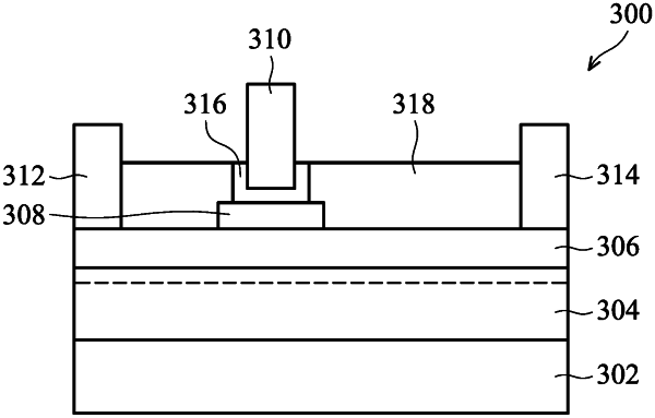
| CPC H01L 29/7787 (2013.01) [H01L 29/1054 (2013.01); H01L 29/2003 (2013.01); H01L 29/42364 (2013.01); H01L 29/66462 (2013.01); H01L 29/7786 (2013.01); H01L 29/205 (2013.01)] | 11 Claims |

|
1. A semiconductor device, comprising: a substrate;
a first III-V compound layer disposed on the substrate;
a second III-V compound layer disposed on the first III-V compound layer;
a p-type doped III-V compound layer disposed on and covering only a portion of the second III-V compound layer;
a passivation layer disposed on the second III-V compound layer and over a part of the p-type doped III-V compound layer;
a gate disposed over the p-type doped III-V compound layer;
a source and a drain disposed on opposite sides of the gate; and
a dielectric layer disposed between the p-type doped III-V compound layer and the gate and further disposed between the passivation layer and the gate,
wherein an uppermost surface of the dielectric layer and an upper surface of the passivation layer are coplanar, the p-type doped III-V compound layer extends beyond the dielectric layer in a direction parallel to the upper surface of the passivation layer, an uppermost surface of the gate is higher than the upper surface of the passivation layer, and the gate does not overlap the passivation layer in a direction perpendicular to the upper surface of the passivation layer.
|