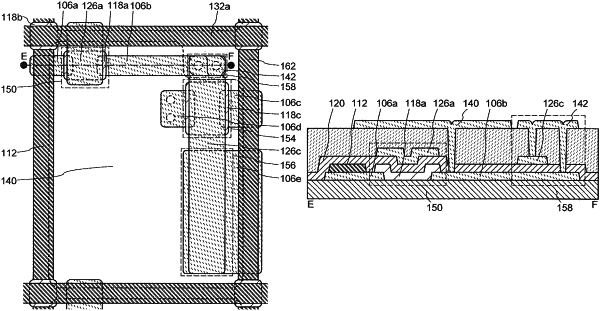
| CPC H01L 29/66969 (2013.01) [H01L 27/1214 (2013.01); H01L 27/1225 (2013.01); H01L 27/124 (2013.01); H01L 27/1288 (2013.01); H01L 29/26 (2013.01); H01L 29/458 (2013.01); H01L 29/4908 (2013.01); H01L 29/78633 (2013.01); H01L 29/7869 (2013.01)] | 7 Claims |

|
1. A display device comprising:
a first conductive layer;
a second conductive layer;
an oxide semiconductor layer over and in contact with the first conductive layer and the second conductive layer, the oxide semiconductor layer comprising a channel formation region of a first transistor;
a third conductive layer over the oxide semiconductor layer, the third conductive layer comprising a gate electrode of the first transistor;
a first insulating layer over the third conductive layer;
a fourth conductive layer over the first insulating layer, the fourth conductive layer being electrically connected to the second conductive layer;
a fifth conductive layer electrically connected to the fourth conductive layer, the fifth conductive layer comprising a first electrode of a capacitor;
a sixth conductive layer comprising a second electrode of the capacitor under the fifth conductive layer; and
a seventh conductive layer comprising a power supply line,
wherein the first insulating layer is over the fifth conductive layer, and
wherein the sixth conductive layer is electrically connected to the seventh conductive layer.
|