| CPC H01L 29/6656 (2013.01) [H01L 21/7682 (2013.01); H01L 21/76897 (2013.01); H01L 21/823468 (2013.01); H01L 29/0649 (2013.01); H01L 29/41775 (2013.01); H01L 29/41791 (2013.01); H01L 29/4991 (2013.01); H01L 29/6653 (2013.01); H01L 29/66545 (2013.01); H01L 29/66795 (2013.01); H01L 29/785 (2013.01); H01L 29/0653 (2013.01)] | 20 Claims |

|
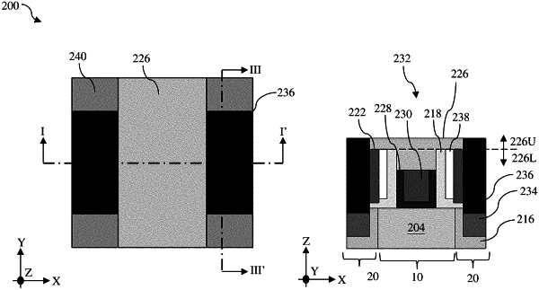
1. A method, comprising:
receiving a substrate, the substrate comprising an active region including a channel region and a source/drain feature adjacent the channel region;
forming a dummy gate stack over the active region;
forming spacers along sidewalls of the dummy gate stack;
removing portions of the spacers that are directly over the active region;
forming a first dummy spacer layer over the dummy gate stack and the source/drain feature;
forming a second dummy spacer layer over the first dummy spacer layer and the source/drain feature;
recessing the second dummy spacer layer to expose top-facing surfaces of the first dummy spacer layer while sidewalls of the first dummy spacer layer remain covered by the second dummy spacer layer;
depositing an etch stop layer over the first dummy spacer layer and the second dummy spacer layer;
depositing an interlayer dielectric layer over the etch stop layer;
replacing the dummy gate stack with a gate structure;
recessing the gate structure, the first dummy spacer layer, the second dummy spacer layer, and the etch stop layer to form a self-aligned contact (SAC) opening;
forming a dielectric feature in the SAC opening;
forming a contact feature extending through the etch stop layer, the interlayer dielectric layer, and the first dummy spacer layer to be in contact with the source/drain feature;
selectively recessing the interlayer dielectric layer and the etch stop layer without substantially etching the dielectric feature and the contact feature to form an opening adjacent the contact feature and to expose a portion of the second dummy spacer layer; and
selectively removing the second dummy spacer layer to form an air gap.
|
|
10. A method, comprising:
receiving a workpiece, the workpiece comprising a channel region and a source/drain feature adjacent the channel region;
forming a dummy gate stack over the channel region;
forming a first spacer layer over the dummy gate stack and the source/drain feature;
forming a second spacer layer over the first spacer layer and the source/drain feature;
recessing the second spacer layer to expose top-facing surfaces of the first spacer layer while sidewalls of the first spacer layer remain covered by the second spacer layer;
depositing an etch stop layer on exposed surfaces of the first and second spacer layers;
depositing an interlayer dielectric layer over the etch stop layer;
planarizing the workpiece to expose the dummy gate stack such that top surfaces of the interlayer dielectric layer, the etch stop layer, the second spacer layer, and the first spacer layer are coplanar;
replacing the dummy gate stack with a gate structure;
recessing the gate structure, the first spacer layer, the second spacer layer, and the etch stop layer to form a contact opening; and
forming a dielectric feature in the contact opening to cover top surfaces of the recessed etch stop layer, second spacer layer, first spacer layer, and gate structure.
|
|
18. A method, comprising:
receiving a workpiece, the workpiece comprising a channel region and a source/drain feature adjacent the channel region;
forming a dummy gate stack over the channel region;
forming a first spacer layer over the dummy gate stack and the source/drain feature;
forming a second spacer layer over the first spacer layer and the source/drain feature;
recessing the second spacer layer to expose top-facing surfaces of the first spacer layer while sidewalls of the first spacer layer remain covered by the second spacer layer;
depositing an etch stop layer on exposed surfaces of the first and second spacer layers;
depositing an interlayer dielectric layer over the etch stop layer;
planarizing the workpiece to expose top surfaces of the dummy gate stack, the interlayer dielectric layer, the etch stop layer, the second spacer layer, and the first spacer layer;
replacing the dummy gate stack with a gate structure;
recessing a portion of the workpiece such that the gate structure is recessed at a faster rate than that of the first spacer layer, the second spacer layer, and the etch stop layer;
forming a capping layer over top surfaces of the recessed etch stop layer, second spacer layer, first spacer layer, and gate structure;
etching through a first portion of the interlayer dielectric layer to form a contact opening exposing the source/drain feature;
forming a contact feature in the contact opening;
selectively recessing a second portion of the interlayer dielectric layer adjacent to the contact feature to expose a portion of the etch stop layer;
selectively etching the exposed portion of the etch stop layer to expose the second spacer layer; and
selectively removing the second spacer layer to form an air gap.
|