| CPC H01L 29/66545 (2013.01) [H01L 21/02532 (2013.01); H01L 21/02636 (2013.01); H01L 21/0337 (2013.01); H01L 21/28247 (2013.01); H01L 21/28518 (2013.01); H01L 21/28568 (2013.01); H01L 21/3086 (2013.01); H01L 21/31105 (2013.01); H01L 21/31144 (2013.01); H01L 21/76224 (2013.01); H01L 21/76232 (2013.01); H01L 21/76801 (2013.01); H01L 21/76802 (2013.01); H01L 21/76816 (2013.01); H01L 21/76834 (2013.01); H01L 21/76846 (2013.01); H01L 21/76849 (2013.01); H01L 21/76877 (2013.01); H01L 21/76897 (2013.01); H01L 21/823431 (2013.01); H01L 21/823481 (2013.01); H01L 21/823807 (2013.01); H01L 21/823814 (2013.01); H01L 21/823821 (2013.01); H01L 21/823828 (2013.01); H01L 21/823842 (2013.01); H01L 21/823857 (2013.01); H01L 21/823871 (2013.01); H01L 21/823878 (2013.01); H01L 23/5226 (2013.01); H01L 23/528 (2013.01); H01L 23/5283 (2013.01); H01L 23/53209 (2013.01); H01L 23/53238 (2013.01); H01L 23/53266 (2013.01); H01L 23/5329 (2013.01); H01L 27/0207 (2013.01); H01L 27/0886 (2013.01); H01L 27/0922 (2013.01); H01L 27/0924 (2013.01); H01L 28/20 (2013.01); H01L 28/24 (2013.01); H01L 29/0649 (2013.01); H01L 29/0653 (2013.01); H01L 29/0847 (2013.01); H01L 29/165 (2013.01); H01L 29/167 (2013.01); H01L 29/41783 (2013.01); H01L 29/41791 (2013.01); H01L 29/516 (2013.01); H01L 29/6653 (2013.01); H01L 29/6656 (2013.01); H01L 29/66636 (2013.01); H01L 29/66795 (2013.01); H01L 29/66818 (2013.01); H01L 29/7843 (2013.01); H01L 29/7845 (2013.01); H01L 29/7846 (2013.01); H01L 29/7848 (2013.01); H01L 29/785 (2013.01); H01L 29/7851 (2013.01); H01L 29/7854 (2013.01); H10B 10/12 (2023.02); H01L 21/02164 (2013.01); H01L 21/0217 (2013.01); H01L 21/0332 (2013.01); H01L 21/76883 (2013.01); H01L 21/76885 (2013.01); H01L 21/823437 (2013.01); H01L 21/823475 (2013.01); H01L 24/16 (2013.01); H01L 24/32 (2013.01); H01L 24/73 (2013.01); H01L 29/665 (2013.01); H01L 29/7842 (2013.01); H01L 29/7853 (2013.01); H01L 2224/16227 (2013.01); H01L 2224/32225 (2013.01); H01L 2224/73204 (2013.01)] | 20 Claims |

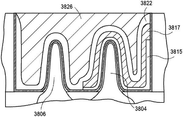
|
1. An integrated circuit structure, comprising:
an inter-layer dielectric layer having a trench therein, the trench having a sidewall;
a semiconductor substrate having a semiconductor fin protruding therefrom and extending into the trench in the inter-layer dielectric layer;
a trench isolation layer on the semiconductor substrate around a lower portion of the semiconductor fin, wherein an upper portion of the semiconductor fin extends above the trench isolation layer;
a gate dielectric over the upper portion of the semiconductor fin, the gate dielectric having a portion laterally spaced apart from the semiconductor fin and along the sidewall of the trench in the inter-layer dielectric layer;
a conductive layer over the gate dielectric, the conductive layer comprising titanium, nitrogen and oxygen, and a portion of the conductive layer in contact with the portion of the gate dielectric laterally spaced apart from the semiconductor fin;
a P-type metal gate layer over the conductive layer, the P-type metal gate layer having an uppermost surface above an uppermost surface of the conductive layer, and a portion of the P-type metal gate layer in contact with the portion of the gate dielectric laterally spaced apart from the semiconductor fin;
an N-type metal gate layer over the P-type metal gate layer, a portion of the N-type metal gate layer in contact with the portion of the gate dielectric laterally spaced apart from the semiconductor fin; and
a conductive fill over the N-type metal gate layer.
|
|
12. A computing device, comprising:
a board; and
a component coupled to the board, the component including an integrated circuit structure, comprising:
an inter-layer dielectric layer having a trench therein, the trench having a sidewall;
a semiconductor substrate having a semiconductor fin protruding therefrom and extending into the trench in the inter-layer dielectric layer;
a trench isolation layer on the semiconductor substrate around a lower portion of the semiconductor fin, wherein an upper portion of the semiconductor fin extends above the trench isolation layer;
a gate dielectric over the upper portion of the semiconductor fin, the gate dielectric having a portion laterally spaced apart from the semiconductor fin and along the sidewall of the trench in the inter-layer dielectric layer;
a conductive layer over the gate dielectric, the conductive layer comprising titanium, nitrogen and oxygen, and a portion of the conductive layer in contact with the portion of the gate dielectric laterally spaced apart from the semiconductor fin;
a P-type metal gate layer over the conductive layer, the P-type metal gate layer having an uppermost surface above an uppermost surface of the conductive layer, and a portion of the P-type metal gate layer in contact with the portion of the gate dielectric laterally spaced apart from the semiconductor fin;
an N-type metal gate layer over the P-type metal gate layer, a portion of the N-type metal gate layer in contact with the portion of the gate dielectric laterally spaced apart from the semiconductor fin; and
a conductive fill over the N-type metal gate layer.
|