| CPC H01L 29/66515 (2013.01) [H01L 21/823821 (2013.01); H01L 21/823871 (2013.01); H01L 27/0924 (2013.01); H01L 29/45 (2013.01); H01L 29/66795 (2013.01); H01L 29/7851 (2013.01); H10B 10/12 (2023.02)] | 20 Claims |

|
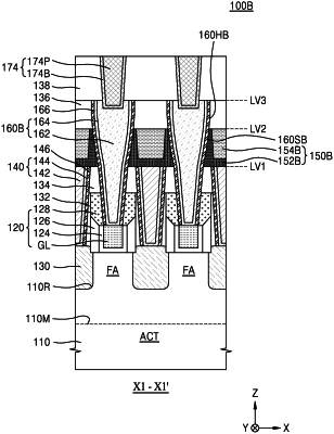
1. A method of forming an integrated circuit device comprising:
forming a gate structure and a source/drain region on a substrate, wherein the source/drain region is on a first side of the gate structure;
forming an interlayer dielectric on the substrate to overlap the gate structure and the source/drain region;
forming a first contact hole that penetrates the interlayer dielectric to expose an upper surface of the source/drain region;
forming a first contact in a lower portion of the first contact hole, wherein the first contact is in contact with the upper surface of the source/drain region;
laterally expanding the first contact hole by removing a portion of the interlayer dielectric surrounding the first contact hole in a plan view to form an enlarged upper region;
forming a contact capping layer in the enlarged upper region;
forming a second contact hole that penetrates the interlayer dielectric to expose an upper surface of the gate structure, wherein a sidewall of the contact capping layer is exposed to an inner wall of the second contact hole; and
forming a second contact in the second contact hole, wherein the second contact is in contact with the upper surface of the gate structure.
|