| CPC H01L 29/4966 (2013.01) [H01L 21/28088 (2013.01); H01L 21/28568 (2013.01); H01L 21/823821 (2013.01); H01L 21/823842 (2013.01); H01L 27/0924 (2013.01); H01L 29/0669 (2013.01); H01L 29/66545 (2013.01); H01L 29/66795 (2013.01); H01L 29/7851 (2013.01); H01L 29/517 (2013.01)] | 20 Claims |

|
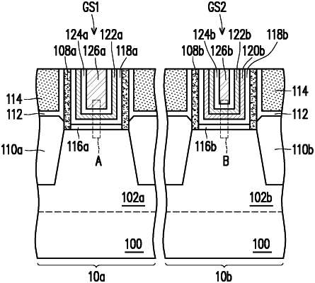
1. A method of forming a FinFET device, comprising:
providing a substrate, the substrate having at least one first fin in a first region and at least one second fin in a second region;
forming first and second dummy gate strips across the first and the second fins and forming a dielectric layer aside the first and second dummy gate strips;
removing the first and second dummy gate strips to form first and second gate trenches in the dielectric layer;
forming a high-k material layer on surfaces of the first and second gate trenches in the first and second regions;
forming a P-type work function metal material layer on the high-k material layer in the first and second regions;
removing the P-type work function metal material layer from the first region;
forming an N-type work function metal material layer in the first and second regions; and
forming a barrier material layer on the N-type work function metal material layer in the first and second regions, wherein forming the barrier material layer comprises:
(a) introducing a titanium precursor, an aluminum precursor and a nitrogen precursor into a process chamber to form a first film;
(b) introducing the titanium precursor and the nitrogen precursor into the process chamber to form a second film; and
(c) repeating step (a) and step (b) alternately m times, wherein m is an integer between 1 and 5,
wherein the barrier material layer is formed with first films and second films alternately stacked, and the first films have a gradient aluminum content ranging from 10 at % to 90 at %.
|