| CPC H01L 29/4236 (2013.01) [H01L 21/76877 (2013.01); H01L 21/823437 (2013.01); H01L 21/82345 (2013.01); H01L 29/42364 (2013.01); H01L 29/4916 (2013.01); H01L 29/518 (2013.01); H01L 29/78 (2013.01); H01L 29/7827 (2013.01)] | 18 Claims |

|
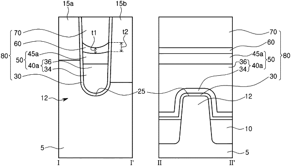
1. A semiconductor device comprising:
a substrate;
a gate trench in the substrate;
a gate insulating film in the gate trench;
a titanium nitride (TiN)-lower gate electrode film on the gate insulating film, the titanium nitride (TiN)-lower gate electrode film including a top surface, a first side surface, and a second side surface opposite the first side surface;
a polysilicon-upper gate electrode film on the titanium nitride (TiN)-lower gate electrode film; and
a gate capping film on the polysilicon-upper gate electrode film,
wherein a center portion of the top surface of the titanium nitride (TiN)-lower gate electrode film overlaps a center portion of the polysilicon-upper gate electrode film in a direction that is perpendicular to a top surface of the substrate,
each of the first side surface and the second side surface of the titanium nitride (TiN)-lower gate electrode film is connected to the gate insulating film,
a top surface of the polysilicon-upper gate electrode film is concave, and
a bottom surface of the gate capping film is convex.
|