| CPC H01L 29/41791 (2013.01) [H01L 21/823431 (2013.01); H01L 21/823437 (2013.01); H01L 21/823462 (2013.01); H01L 21/823468 (2013.01); H01L 29/0673 (2013.01); H01L 29/41733 (2013.01); H01L 29/4236 (2013.01); H01L 29/42392 (2013.01); H01L 29/66439 (2013.01); H01L 29/66545 (2013.01); H01L 29/66795 (2013.01); H01L 29/775 (2013.01); H01L 29/7854 (2013.01); H01L 29/7855 (2013.01); H01L 29/78696 (2013.01); H01L 29/4966 (2013.01); H01L 29/7848 (2013.01)] | 20 Claims |

|
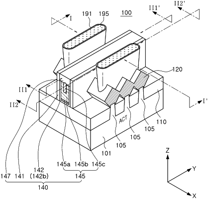
1. A method of manufacturing a semiconductor device, the method comprising:
forming an active fin on a substrate, the active fin extending in a first direction;
forming a dummy gate structure to cover the active fin on a substrate, the dummy gate structure extending a second direction intersecting the first direction;
forming a pair of gate spacers on both sides of the dummy gate structure, the pair of gate spacers extending in the second direction;
removing the dummy structure to form a trench extending in the second direction between the pair of gate spacers;
forming a gate insulating film on an upper surface and lateral surfaces of the active fin and on inner sidewalls of the pair of gate spacers in the trench;
forming a first gate electrode on a first portion of the gate insulating film corresponding to the upper surface and the lateral surfaces of the active fin, the first gate electrode not disposed on second and third portions of the gate insulating film corresponding to the inner sidewalls of the pair of gate spacers, respectively; and
forming a second gate electrode on the first gate electrode and on the second and third portions of the gate insulating film.
|