| CPC H01L 29/408 (2013.01) [H01L 21/0217 (2013.01); H01L 21/02186 (2013.01); H01L 21/28575 (2013.01); H01L 23/291 (2013.01); H01L 23/3192 (2013.01); H01L 29/2003 (2013.01); H01L 29/205 (2013.01); H01L 29/452 (2013.01); H01L 29/66462 (2013.01); H01L 29/7786 (2013.01); H01L 29/7787 (2013.01)] | 12 Claims |

|
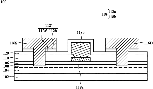
1. A semiconductor structure, comprising:
a substrate;
a buffer layer disposed on the substrate;
a barrier layer disposed on the buffer layer;
a dielectric layer disposed on the barrier layer;
a protection layer disposed on the dielectric layer, wherein the protection layer is a multilayer structure, and wherein the protection layer comprises:
a material layer, wherein the material layer comprises SiN; and
a passivation layer disposed on the material layer; and
a source structure and a drain structure both disposed directly above the protection layer, wherein sidewalls of the protection layer are aligned with uppermost-outermost opposing sidewalls of each of the source structure and the drain structure and aligned with lowermost-outermost opposing sidewalls of each of the source structure and the drain structure, and the protection layer is above the dielectric layer and below one of the source structure and the drain structure, and wherein the protection layer is solely under the source structure and the drain structure,
wherein a vertical projection of an entirety of protrusions of the source structure and of protrusions of an entirety of the drain structure on the substrate and a vertical projection of an entirety of the protection layer on the substrate have a same entire projection area.
|