| CPC H01L 29/0692 (2013.01) [B82Y 10/00 (2013.01); H01L 21/823431 (2013.01); H01L 21/845 (2013.01); H01L 27/0886 (2013.01); H01L 27/1211 (2013.01); H01L 29/0649 (2013.01); H01L 29/0653 (2013.01); H01L 29/0847 (2013.01); H01L 29/1037 (2013.01); H01L 29/1608 (2013.01); H01L 29/161 (2013.01); H01L 29/165 (2013.01); H01L 29/41791 (2013.01); H01L 29/4966 (2013.01); H01L 29/517 (2013.01); H01L 29/66795 (2013.01); H01L 29/7848 (2013.01); H01L 29/785 (2013.01); H01L 29/775 (2013.01)] | 19 Claims |

|
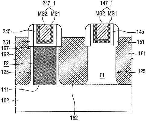
1. A semiconductor device comprising:
a first channel active pattern protruding from a substrate and extending in a first direction;
a second channel active pattern protruding from the substrate and extending in the first direction, wherein the first and second channel active patterns are separated from one another in the first direction;
a field insulation layer disposed on the substrate;
a source/drain region between the first channel active pattern and the field insulation layer;
a first gate pattern disposed on the first channel active pattern and including a first gate and a first gate spacer; and
a second gate pattern disposed on the field insulation layer and including a second gate and a second gate spacer,
wherein a bottom of the second gate is higher than a lowermost part of the source/drain region,
wherein a bottom of the field insulation layer is lower than the lowermost part of the source/drain region, and
wherein the second gate vertically overlaps a portion of the first channel active pattern.
|