| CPC H01L 28/65 (2013.01) [H01L 23/5223 (2013.01); H01L 28/87 (2013.01)] | 7 Claims |

|
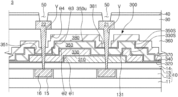
1. A metal-insulator-metal capacitor, comprising:
N electrodes stacked on a substrate, where N is a plural integer, wherein each nth electrode covers an upper surface and a side surface of an n−1 electrode stacked therebelow, where n is an integer of 1 to N; and
M dielectric layers respectively interposed between the N electrodes, each mth dielectric layer covering upper surfaces and side surfaces of each nth electrode, where M=N−1 and m is an integer from 1 to M,
wherein a first dielectric layer among the M dielectric layers covers a top surface of the first electrode among the N electrodes, a side surface of the first electrode, and a top surface portion of the substrate adjacent the side surface of the first electrode,
wherein each of the second to Mth dielectric layers among the M dielectric layers covers the top surface of the respective second to N−1th electrodes, the side surface of the respective second to N−1th electrodes, and a top surface portion of the respective first to M−1 dielectric layers adjacent the side surface of the respective second to N−1th electrodes, wherein portions of the M dielectric layers extend parallel to the top surface of the substrate and are sequentially stacked over the top surface of the substrate to define a stack of parallel extending portions of the M dielectric layers, and
wherein one side region of the Nth electrode has a staircase structure with N−1 bent portions defining N−1 stairs of the staircase structure, and a bottom surface of a lowermost stair among the N−1 stairs is in direct contact with an uppermost surface of the stack of parallel extending portions of the M dielectric layers.
|