| CPC H01L 27/156 (2013.01) [H01L 33/005 (2013.01); H01L 33/42 (2013.01); H01L 33/44 (2013.01); H01L 2933/0016 (2013.01); H01L 2933/0025 (2013.01)] | 2 Claims |

|
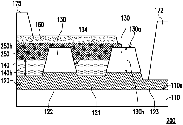
1. A manufacturing method of a light-emitting apparatus, comprising:
forming a first light-emitting device by a substrate, wherein the first light-emitting device comprises:
a first type semiconductor layer;
a patterned insulating layer, covering the first type semiconductor layer and having a plurality of first insulating openings, wherein the plurality of first insulating openings are separated from each other;
a first light-emitting layer, located in the plurality of first insulating openings and covering a portion of the first type semiconductor layer; and
a second type semiconductor layer, located on the first light-emitting layer; and
disposing the first light-emitting device on a circuit substrate to electrically connect the circuit substrate, wherein the manufacturing the method of the light-emitting apparatus, further comprising: forming a second light-emitting device by the substrate, wherein the second light-emitting device comprises: the first type semiconductor layer; the patterned insulating layer, further having a plurality of second insulating openings, wherein the plurality of second insulating openings are separated from each other; a second light-emitting layer, located in the plurality of second insulating openings and covering a portion of the first type semiconductor layer; and the second type semiconductor layer, located on the second light-emitting layer, wherein apertures of the plurality of second insulating openings are different from apertures of the plurality of first insulating openings; and/or a pitch between the adjacent plurality of first insulating openings is different from a pitch between the adjacent plurality of second insulating openings; and disposing the second light-emitting device on the circuit substrate to electrically connect the circuit substrate; and simultaneously transferring the first light-emitting device and the second light-emitting device formed by the substrate to a transfer substrate.
|