| CPC H01L 27/156 (2013.01) [H01L 33/005 (2013.01); H01L 33/0093 (2020.05); H01L 33/382 (2013.01); H01L 33/62 (2013.01); H01L 2933/0016 (2013.01); H01L 2933/0066 (2013.01)] | 16 Claims |

|
1. A fabrication method of a display device, comprising:
providing a light emitting diode (LED) display device, wherein the LED display device comprising:
a circuit substrate; and
a plurality of first LEDs, respectively disposed corresponding to a plurality of first placement regions of the circuit substrate, and the plurality of first LEDs are electrically connected to the circuit substrate;
a plurality of second LEDs respectively disposed corresponding to a plurality of second placement regions of the circuit substrate;
detecting the LED display device, wherein the plurality of second LEDs are faulty;
removing the plurality of second LEDs from the circuit substrate;
providing a plurality of LED substrates, each of the plurality of LED substrates comprises at least one of third LEDs;
providing a plurality of first transferring substrates, and providing a support structure for fixing one of the plurality of first transferring substrates;
respectively transferring the at least one of third LEDs of each of the plurality of LED substrates to a corresponding one of the plurality of first transferring substrates based on positions of the plurality of second placement regions, wherein when transferring the at least one of third LEDs of one of the plurality of LED substrates to the one of the plurality of first transferring substrates, the support structure is laterally surrounding and separated from the one of the plurality of LED substrates, and wherein the support structure and the one of the plurality of LED substrates are located on a same side of the one of the plurality of first transferring substrates;
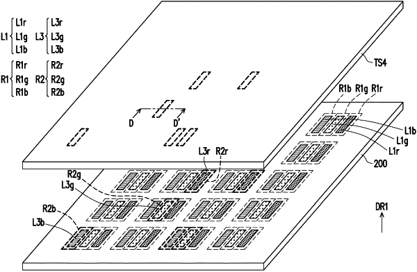
transferring the at least one of third LEDs on each of the plurality of first transferring substrates to a same second transferring substrate;
overlapping the second transferring substrate with the circuit substrate, wherein a plurality of third LEDs are located on a side of the second transferring substrate facing the circuit substrate, wherein positions of the plurality of third LEDs overlap the plurality of second placement regions; and
electrically connecting the plurality of third LEDs on the second transferring substrate to the circuit substrate.
|