| CPC H01L 27/15 (2013.01) [H01L 25/0753 (2013.01); H01L 27/1214 (2013.01); H01L 33/60 (2013.01); H01L 33/62 (2013.01); H01L 2933/0066 (2013.01)] | 15 Claims |

|
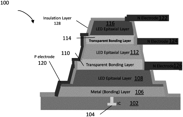
1. A single pixel multi-color micro light-emitting diode (LED) device for a display panel, comprising:
a substrate supporting a pixel driver;
a first LED structure layer stacked on top of the substrate;
a second LED structure layer stacked on top of the first LED structure layer; and
a metal bonding layer between the substrate and the first LED structure layer,
wherein the first LED structure layer and the second LED structure layer substantially overlap laterally with one another to form a light path that combines light emitted from the first LED structure layer and the second LED structure layer,
wherein each of the first and second LED structure layers comprises:
an epitaxial structure forming an LED;
a lower conductive layer electrically connected to a bottom of the LED; and
an upper transparent conductive layer electrically connected to a top of the LED,
wherein:
the lower conductive layer of the first LED structure layer and the lower conductive layer of the second LED structure layer are electrically connected to the pixel driver through a first-type electrode metal contact pad layer and the metal bonding layer, wherein the first-type electrode metal contact pad layer is in direct contact with the lower conductive layer of the first LED structure layer and the lower conductive layer of the second LED structure layer;
the upper transparent conductive layer of the first LED structure layer is electrically connected to a first second-type electrode metal contact pad; and
the upper transparent conductive layer of the second LED structure layer is electrically connected to a second second-type electrode metal contact pad.
|