| CPC H01L 27/1464 (2013.01) [G01J 1/44 (2013.01); H01L 27/14621 (2013.01); H01L 27/14627 (2013.01); H01L 27/14629 (2013.01); H01L 27/1463 (2013.01); H01L 27/14634 (2013.01); H01L 27/14636 (2013.01); H01L 27/14685 (2013.01); H04N 25/70 (2023.01); G01J 2001/448 (2013.01)] | 20 Claims |

|
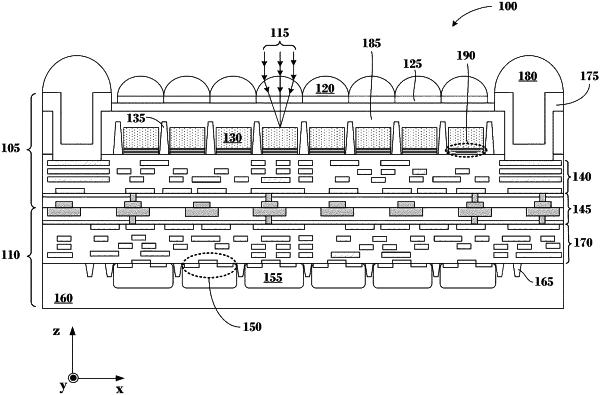
1. An image-sensing structure, comprising:
a stack structure, comprising:
a first layer with a first refractive index and a first thickness substantially equal to one fourth of a wavelength of an incident radiation divided by the first refractive index; and
a second layer with a second refractive index different from the first refractive index and a second thickness substantially equal to one fourth of the wavelength of the incident radiation divided by the second refractive index;
a radiation-sensing region comprising a first epitaxial layer disposed on the stack structure;
a second epitaxial layer in contact with a sidewall and a top surface of the radiation-sensing region; and
an implant layer in contact with a sidewall and a top surface of the second epitaxial layer.
|