| CPC H01L 27/14636 (2013.01) [H01L 23/481 (2013.01); H01L 24/08 (2013.01); H01L 27/14634 (2013.01); H01L 2224/08145 (2013.01)] | 12 Claims |

|
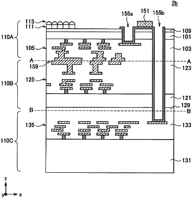
1. An imaging device, comprising:
a first substrate, including:
a first semiconductor substrate including a plurality of pixels;
a first multi-layered wiring layer stacked on the first semiconductor substrate; and
a first electrode included in the first multi-layered wiring layer;
a second substrate, including:
a second semiconductor substrate;
a second multi-layered wiring layer stacked on the second semiconductor substrate;
a second electrode included in the second multi-layered wiring layer;
an insulating layer on a second side of the second semiconductor substrate, wherein the second substrate is stacked on the first substrate such that the first multi-layered wiring layer and the second multi-layered wiring layer are opposed to each other;
a third electrode included in the insulating layer; and
a via, wherein the via extends from the second multi-layered wiring layer, through the second semiconductor substrate and to the insulating layer, and
wherein the via is electrically connected to the third electrode; and
a third substrate, including:
a third semiconductor substrate;
a third multi-layered wiring layer stacked on the third semiconductor substrate; and
a fourth electrode included in the third multi-layered wiring layer, wherein the third substrate is stacked on the second substrate such that the insulating layer and the third multi-layered wiring layer are opposed to each other,
wherein the first substrate and the second substrate are electrically connected by a direct contact between the first electrode and the second electrode at a bonding surface between the first substrate and the second substrate,
wherein the second substrate and the third substrate are electrically connected by a direct contact between the third electrode and the fourth electrode at a bonding surface between the second substrate and the third substrate,
wherein, in a plan view, at least a part of the via overlaps at least a part of the third electrode and at least a part of the fourth electrode, and
wherein the third substrate includes a logic circuit.
|