| CPC H01L 27/0924 (2013.01) [H01L 21/823431 (2013.01); H01L 21/823821 (2013.01); H01L 27/0207 (2013.01); H01L 27/0886 (2013.01); H01L 29/41791 (2013.01); H01L 2027/11812 (2013.01); H01L 2027/11831 (2013.01); H01L 2027/11861 (2013.01); H01L 2027/11864 (2013.01); H01L 2027/11875 (2013.01); H01L 2027/11887 (2013.01)] | 20 Claims |

|
1. A method, comprising:
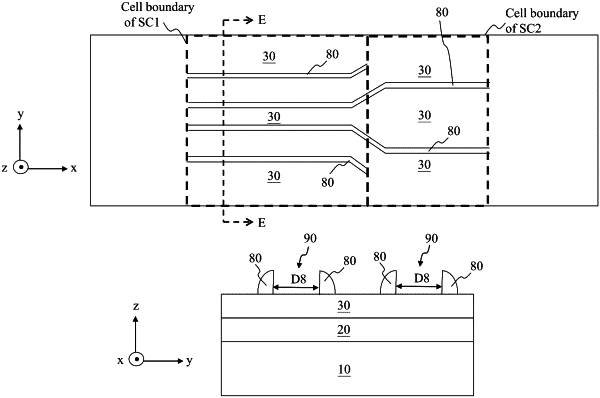
forming a patterned sacrificial layer over a first circuit region of a substrate and a second circuit region of the substrate, the patterned sacrificial layer extending lengthwise along a first direction, wherein a longitudinal axis of the patterned sacrificial layer in the first circuit region is offset in a second direction relative to a longitudinal axis of the patterned sacrificial layer in the second circuit region, the second direction being generally perpendicular to the first direction;
forming spacers on sidewalls of the patterned sacrificial layer;
removing the patterned sacrificial layer, wherein the spacers remain over the first circuit region and the second circuit region of the substrate after the removing of the patterned sacrificial layer;
removing selective portions of the spacers disposed over the second circuit region to form a patterned spacer layer; and
etching the substrate using the patterned spacer layer as an etch mask to form a plurality of fin lines in the first circuit region of the substrate and a single fin line in the second circuit region of the substrate, wherein a projection of a longitudinal axis of the single fin line along the first direction lies in a space separating adjacent ones of the plurality of fin lines, and wherein a projection of each longitudinal edge of the single fin line along the first direction lies in the space.
|