| CPC H01L 27/0886 (2013.01) [H01L 21/823431 (2013.01); H01L 21/823821 (2013.01); H01L 27/0924 (2013.01); H01L 29/1037 (2013.01); H01L 29/42372 (2013.01); H01L 29/66545 (2013.01); H01L 29/66818 (2013.01); H01L 29/7848 (2013.01); H01L 29/785 (2013.01)] | 20 Claims |

|
1. A semiconductor device, comprising:
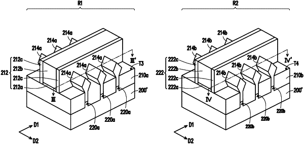
a semiconductor substrate having a first region and a second region, wherein the first region comprises a first semiconductor fin and the second region comprises a second semiconductor fin, a width of a middle portion of the first semiconductor fin is equal to widths of end portions of the first semiconductor fin, a width of a middle portion of the second semiconductor fin is different from widths of end portions of the second semiconductor fin, a dopant of the first semiconductor fin and the second semiconductor fin comprises boron, BF2, phosphorus, arsenic, or a combination thereof, a dopant concentration within the first semiconductor fin ranges from 2×10¹¹ atom/cm2 to 1×10¹² atom/cm2 and a dopant concentration within the first semiconductor fin is less than the dopant concentration within the second semiconductor fin;
a plurality of gate stacks over a portion of the first semiconductor fin and a portion of the second semiconductor fin;
a first S/D covering another portion of the first semiconductor fin; and
a second S/D covering another portion of the second semiconductor fin.
|