| CPC H01L 27/0733 (2013.01) [H01L 23/3128 (2013.01); H01L 23/5226 (2013.01); H01L 24/09 (2013.01); H01L 24/17 (2013.01); H05K 1/0231 (2013.01); H01L 2924/15311 (2013.01); H05K 2201/09118 (2013.01)] | 43 Claims |

|
1. An apparatus, comprising:
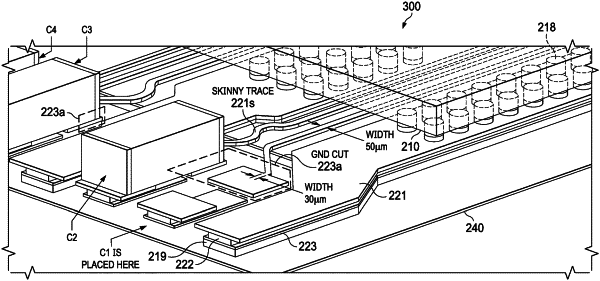
a multi-layer molded interconnect substrate (MIS) having a signal layer including first and second traces for a first channel and first and second traces for a second channel on a dielectric layer with vias, wherein the first and second traces of the first and second channels include narrowed trace regions and a bottom metal layer comprises a patterned layer including a plurality of ground cut regions, at least one of the first and second traces for the first channel and the first and second traces for the second channel being over one of the ground cut regions.
|