| CPC H01L 27/0727 (2013.01) [H01L 27/0605 (2013.01); H01L 27/0629 (2013.01); H01L 29/2003 (2013.01); H01L 29/42316 (2013.01); H01L 29/7786 (2013.01); H03K 17/04123 (2013.01); H03K 17/08122 (2013.01); H03K 17/302 (2013.01)] | 35 Claims |

|
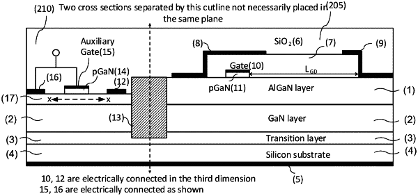
1. A III-nitride power semiconductor based heterojunction device, comprising:
an active heterojunction transistor formed on a substrate, the active heterojunction transistor comprising:
a first III-nitride semiconductor region comprising a first heterojunction comprising an active two dimensional carrier gas of second conductivity type;
a first terminal operatively connected to the III-nitride semiconductor region;
a second terminal laterally spaced from the first terminal and operatively connected to the III-nitride semiconductor region;
an active gate region formed over the III-nitride semiconductor region, the active gate region being formed between the first terminal and the second terminal;
an auxiliary heterojunction transistor formed on the said substrate or a further substrate, the auxiliary heterojunction transistor comprising:
a second III-nitride semiconductor region comprising a second heterojunction comprising an auxiliary two dimensional carrier gas of second conductivity type;
a first additional terminal operatively connected to the second III-nitride semiconductor region;
a second additional terminal laterally spaced from the first additional terminal and operatively connected to the second III-nitride semiconductor region;
an auxiliary gate region formed over the second III-nitride semiconductor region, the auxiliary gate region being formed between the first additional terminal and the second additional terminal;
wherein the first additional terminal is operatively connected with the auxiliary gate region, and wherein the second additional terminal is operatively connected with the active gate region; and
wherein the auxiliary heterojunction transistor is a first auxiliary heterojunction transistor, and wherein the heterojunction power device further comprises a second auxiliary heterojunction transistor which is operatively connected in parallel with the first auxiliary transistor, and wherein the first additional terminal of the first auxiliary heterojunction transistor is operatively connected to a source terminal of the second auxiliary heterojunction transistor, and the second additional terminal of the first auxiliary heterojunction transistor is operatively connected to a drain terminal of the second auxiliary heterojunction transistor; and
wherein the heterojunction device comprises a shielding and/or decoupling structure disposed between the active heterojunction transistor and the auxiliary heterojunction transistor.
|