| CPC H01L 27/0664 (2013.01) [H01L 29/7397 (2013.01); H01L 29/8613 (2013.01); H03K 17/567 (2013.01)] | 11 Claims |

|
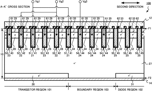
1. A semiconductor device comprising:
a transistor region including
a semiconductor layer having a first face and a second face opposed to the first face,
a first semiconductor region of a first conductivity type provided in the semiconductor layer,
a second semiconductor region of a second conductivity type provided in the semiconductor layer and provided between the first semiconductor region and the first face,
a third semiconductor region of a first conductivity type provided in the semiconductor layer and provided between the second semiconductor region and the first face,
a fourth semiconductor region of a second conductivity type provided in the semiconductor layer and provided between the third semiconductor region and the first face,
a fifth semiconductor region of a first conductivity type provided in the semiconductor layer, provided between the third semiconductor region and the first face, and having a first conductivity type impurity concentration higher than the first conductivity type impurity concentration of the third semiconductor region,
a first trench provided on a side of the first face in the semiconductor layer and in contact with the second semiconductor region, the third semiconductor region, and the fourth semiconductor region,
a first gate electrode provided in the first trench,
a first gate insulating film provided between the first gate electrode and the second semiconductor region, between the first gate electrode and the third semiconductor region, and between the first gate electrode and the fourth semiconductor region,
a second trench provided on a side of the first face in the semiconductor layer and in contact with the second semiconductor region, the third semiconductor region, and the fourth semiconductor region;
a second gate electrode provided in the second trench,
a second gate insulating film provided between the second gate electrode and the second semiconductor region, between the second gate electrode and the third semiconductor region, and between the second gate electrode and the fourth semiconductor region,
a third trench provided on a side of the first face in the semiconductor layer and in contact with the second semiconductor region, the third semiconductor region, and the fourth semiconductor region,
a third gate electrode provided in the third trench,
a third gate insulating film provided between the third gate electrode and the second semiconductor region, between the third gate electrode and the third semiconductor region, and between the third gate electrode and the fourth semiconductor region,
a first electrode provided on a side of the first face with respect to the semiconductor layer and in contact with the fourth semiconductor region and the fifth semiconductor region, and
a second electrode provided on a side of the second face with respect to the semiconductor layer and in contact with the first semiconductor region;
a diode region including
the semiconductor layer,
the second semiconductor region,
a sixth semiconductor region of a second conductivity type provided in the semiconductor layer, provided between the second semiconductor region and the second face, and having a second conductivity type impurity concentration higher than the second conductivity type impurity concentration of the second semiconductor region,
a seventh semiconductor region of a first conductivity type provided in the semiconductor layer and provided between the second semiconductor region and the first face,
an eighth semiconductor region of a first conductivity type provided in the semiconductor layer, provided between the seventh semiconductor region and the first face, and having a first conductivity type impurity concentration higher than the first conductivity type impurity concentration of the seventh semiconductor region,
a fifth trench provided on a side of the first face in the semiconductor layer and in contact with the second semiconductor region and the seventh semiconductor region,
a conductive layer provided in the fifth trench,
an insulating film provided between the conductive layer and the second semiconductor region and between the conductive layer and the seventh semiconductor region,
the first electrode in contact with the eighth semiconductor region, and
the second electrode in contact with the sixth semiconductor region;
a boundary region provided between the transistor region and the diode region, the boundary region including
the semiconductor layer,
the second semiconductor region,
a ninth semiconductor region of a first conductivity type provided in the semiconductor layer and provided between the second semiconductor region and the first face,
a tenth semiconductor region of a second conductivity type provided in the semiconductor layer and provided between the ninth semiconductor region and the first face,
an eleventh semiconductor region of a first conductivity type provided in the semiconductor layer, provided between the ninth semiconductor region and the first face, and having a first conductivity type impurity concentration higher than the first conductivity type impurity concentration of the ninth semiconductor region,
a fourth trench provided on a side of the first face in the semiconductor layer and in contact with the second semiconductor region, the ninth semiconductor region, and the tenth semiconductor region,
a fourth gate electrode provided in the fourth trench,
a fourth gate insulating film provided between the fourth gate electrode and the second semiconductor region, between the fourth gate electrode and the ninth semiconductor region, and between the fourth gate electrode and the tenth semiconductor region,
the first electrode in contact with the tenth semiconductor region and the eleventh semiconductor region, and
the second electrode;
a first electrode pad provided on a side of the first face with respect to the semiconductor layer and electrically connected to the first gate electrode;
a second electrode pad provided on a side of the first face with respect to the semiconductor layer and electrically connected to the second gate electrode; and
a third electrode pad provided on a side of the first face with respect to the semiconductor layer and electrically connected to the third gate electrode and the fourth gate electrode.
|