| CPC H01L 27/0251 (2013.01) [G02F 1/136204 (2013.01); G09G 3/3208 (2013.01); G09G 3/3225 (2013.01); G09G 3/36 (2013.01); G09G 3/3648 (2013.01); H01L 27/1214 (2013.01); G09G 2300/043 (2013.01); G09G 2300/0819 (2013.01); G09G 2330/04 (2013.01); H01L 27/12 (2013.01)] | 20 Claims |

|
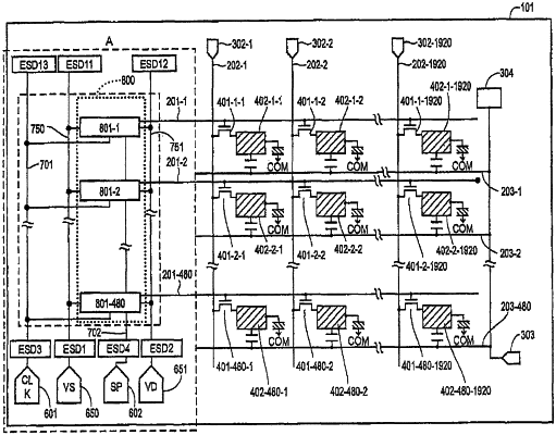
1. A display device comprising:
a substrate;
an active matrix arranged on the substrate;
a driving circuit arranged along a first side of the substrate in a peripheral area that surrounds the active matrix;
in the peripheral area, a first signal line having a first end that is connected between a first terminal and a first end of the driving circuit, the first signal line supplying a first driving signal to the driving circuit;
a first protective circuit arranged in the peripheral area and connected between the first end of the first signal line and the first end of the driving circuit;
a second protective circuit arranged in the peripheral area and connected between a second end of the driving circuit and a second end of the first signal line;
in the peripheral area, a first power line having a third end that is connected between a second terminal and the first end of the driving circuit, the first power line supplying a first driving voltage to the driving circuit;
a third protective circuit arranged in the peripheral area and connected between the third end of the first power line and the first end of the driving circuit; and
a fourth protective circuit arranged in the peripheral area and connected between the second end of the driving circuit and a fourth end of the first power line,
wherein the driving circuit is connected between the first protective circuit and the second protective circuit, and
wherein the driving circuit is connected between the third protective circuit and the fourth protective circuit.
|