| CPC H01L 27/0248 (2013.01) [H01L 27/1207 (2013.01); H01L 29/7436 (2013.01)] | 20 Claims |

|
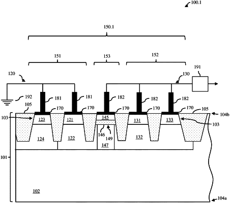
1. A structure comprising:
a hybrid semiconductor substrate comprising bulk semiconductor and semiconductor-on-insulator regions; and
a semiconductor-controlled rectifier comprising:
in a first bulk semiconductor region, a first Pwell and a first Nwell positioned laterally adjacent to the first Pwell;
in a second bulk semiconductor region, a second Nwell electrically connected to an anode terminal; and
in a semiconductor-on-insulator region positioned laterally between the first bulk semiconductor region and the second bulk semiconductor region, a second Pwell positioned laterally between and abutting the first Nwell and the second Nwell, an insulator layer on the second Pwell, and a semiconductor layer on the insulator layer positioned laterally between and abutting trench isolation regions, and electrically connected to the anode terminal.
|