| CPC H01L 27/0207 (2013.01) [G06F 30/00 (2020.01); G11C 5/063 (2013.01); G11C 8/16 (2013.01); G11C 11/412 (2013.01); H01L 21/76895 (2013.01); H01L 27/088 (2013.01); H01L 27/11807 (2013.01); H01L 2027/11875 (2013.01)] | 15 Claims |

|
1. An integrated circuit comprising:
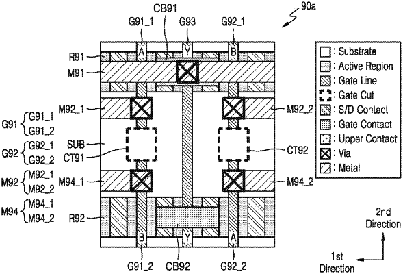
a first active region and a second active region, each extending on a substrate in a first horizontal direction in parallel to each other, wherein the first active region and the second active region have conductivity types different from each other;
a first gate line extending in a second horizontal direction that crosses the first horizontal direction, the first gate line comprising a first partial gate line and a second partial gate line, wherein the first partial gate line forms a first transistor with the first active region and the second partial gate line forms a second transistor with the second active region, wherein the first transistor comprises a gate configured to receive a first input signal, and the second transistor comprises a gate configured to receive a second input signal;
a second gate line extending in the second horizontal direction and comprising a third partial gate line and a fourth partial gate line, wherein the third partial gate line forms a third transistor with the first active region and the fourth partial gate line forms a fourth transistor with the second active region, wherein the third transistor comprises a gate configured to receive the second input signal and the fourth transistor comprises a gate configured to receive the first input signal; and
a first metal line, a second metal line, and a third metal line, each extending on the first and second gate lines in the first horizontal direction, the first, second, and third metal lines extending in parallel to one another,
wherein the first and second partial gate lines are spaced apart from each other in the second horizontal direction,
wherein the third and fourth partial gate lines are spaced apart from each other in the second horizontal direction,
wherein the first metal line comprises a first metal pattern electrically connected to the first partial gate line and a second metal pattern electrically connected to the third partial gate line,
wherein the second metal line comprises a third metal pattern electrically connected to the second partial gate line and a fourth metal pattern electrically connected to the fourth partial gate line, and
wherein the third metal line is electrically connected to drain regions of the first, second, third, and fourth transistors.
|