| CPC H01L 25/18 (2013.01) [H01L 24/08 (2013.01); H10B 41/10 (2023.02); H10B 41/27 (2023.02); H10B 41/35 (2023.02); H10B 41/40 (2023.02); H10B 43/10 (2023.02); H10B 43/27 (2023.02); H10B 43/35 (2023.02); H10B 43/40 (2023.02); H01L 2224/08147 (2013.01); H01L 2924/1431 (2013.01); H01L 2924/1438 (2013.01)] | 20 Claims |

|
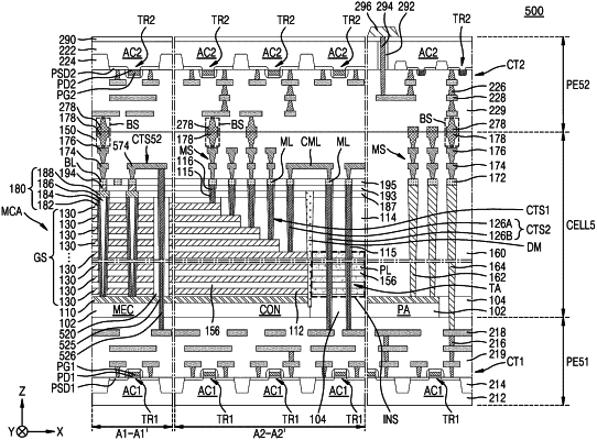
1. A semiconductor device comprising:
a first peripheral circuit region comprising a plurality of lower circuitries;
a second peripheral circuit region apart from the first peripheral circuit region in a vertical direction, the second peripheral circuit region comprising a plurality of upper circuitries; and
a cell region comprising a plurality of word lines, the cell region between the first peripheral circuit region and the second peripheral circuit region in the vertical direction, such that a lower surface of the cell region is on an upper surface of the first peripheral circuit region and lower surface of the second peripheral circuit region is on an upper surface of the cell region,
wherein the plurality of word lines comprise a first word line connected to a first lower circuitry selected from the plurality of lower circuitries and a second word line connected to a first upper circuitry selected from the plurality of upper circuitries.
|