| CPC H01L 25/167 (2013.01) [H01L 25/0753 (2013.01); H01L 25/0756 (2013.01); H01L 27/14645 (2013.01); H01L 27/14647 (2013.01); H01L 27/14667 (2013.01); H01L 27/153 (2013.01); H01L 33/0062 (2013.01); H01L 33/0075 (2013.01); H01L 33/42 (2013.01); H01L 33/62 (2013.01); H10K 59/32 (2023.02); H01L 27/1222 (2013.01); H01L 33/305 (2013.01); H01L 33/325 (2013.01)] | 12 Claims |

|
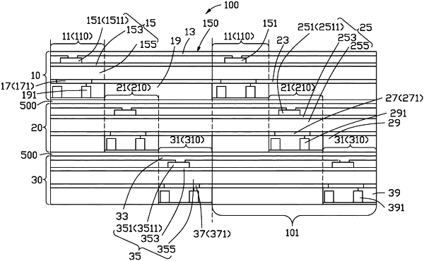
1. A method for making a micro LED display panel, comprising:
forming a blue LED layer, the blue LED layer comprising a plurality of blue micro LEDs spaced apart from each other, each of the plurality of blue micro LEDs defining a blue sub-pixel;
forming a green LED layer, the green LED layer comprising a plurality of green micro LEDs spaced apart from each other, each of the plurality of green micro LEDs defining a green sub-pixel;
forming a red LED layer, the red LED layer comprising a plurality of red micro LEDs spaced apart from each other, each of the plurality of red micro LEDs defining a red sub-pixel; and
stacking the blue LED layer, the green LED layer, and the red LED layer one by one along a direction; wherein each of the plurality of blue micro LEDs, each of the plurality of green micro LEDs, and each of the plurality of red micro LEDs are staggered from each other;
wherein the blue LED layer comprises a first transparent conductive layer, a first light emitting layer, and a first electrode layer stacked one by one along the depth direction; the first light emitting layer is provided between the first transparent conductive layer and the first electrode layer; the first light emitting layer comprises an N-type doped inorganic light emitting layer, an active layer, and a P-type doped inorganic light emitting layer stacked one by one along the depth direction; the active layer is provided between the P-type doped inorganic light emitting layer and the N-type doped inorganic light emitting layer; the N-type doped inorganic light emitting layer comprises a plurality of N-type doped units spaced apart from each other; the first electrode layer comprises a plurality of electrodes spaced apart from each other; each of the plurality of N-type doped units is coupled to the first transparent conductive layer; the P-type doped inorganic light emitting layer is coupled to each of the plurality of electrodes; a projection of each of the plurality of N-type doped units on the first electrode layer overlaps with one of the plurality of electrodes; a portion of the blue LED layer corresponding to one of the plurality of N-type doped units defines one blue sub-pixel.
|