| CPC H01L 25/0652 (2013.01) [H01L 23/5383 (2013.01); H01L 23/5385 (2013.01); H01L 23/5386 (2013.01); H01L 29/42392 (2013.01); H01L 29/785 (2013.01)] | 20 Claims |

|
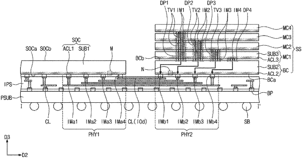
1. A semiconductor package, comprising:
a logic die provided on an interposer substrate; and
a memory stack structure provided adjacent to the logic die,
wherein the memory stack structure comprises:
a buffer die provided on the interposer substrate; and
a plurality of memory dies stacked on the buffer die,
wherein the buffer die comprises an active layer, the active layer comprising:
a first active pattern provided on a first substrate;
a first device isolation layer provided on the first substrate and configured to define the first active pattern; and
a first gate electrode provided on a channel of the first active pattern,
wherein the channel of the first active pattern is positioned higher than an upper surface of the first device isolation layer.
|
|
20. A semiconductor package, comprising:
a logic die provided on an interposer substrate;
a buffer die provided on the interposer substrate; and
a plurality of memory dies provided on the buffer die,
wherein the buffer die comprises an active layer including:
a first active pattern provided on a first substrate;
a first device isolation layer provided on the first substrate; and
a first gate electrode provided on a channel of the first active pattern, and
wherein the channel of the first active pattern is positioned higher than an upper surface of the first device isolation layer.
|