| CPC H01L 24/80 (2013.01) [H01L 24/74 (2013.01); H01L 2224/80123 (2013.01); H01L 2224/80129 (2013.01); H01L 2224/8013 (2013.01); H01L 2224/80895 (2013.01); H01L 2924/1438 (2013.01)] | 20 Claims |

|
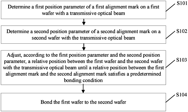
1. A wafer bonding method, comprising:
determining a first position parameter of a first alignment mark on a first wafer by using an optical beam;
determining a second position parameter of a second alignment mark on a second wafer with the optical beam, wherein the optical beam has a property of transmitting through a wafer;
adjusting, according to the first position parameter and the second position parameter, a relative position between the first wafer and the second wafer with the optical beam until a relative position between the first alignment mark and the second alignment mark satisfies a predetermined bonding condition, comprising:
performing a first alignment, comprising: adjusting, according to the first position parameter and the second position parameter, a position of the first wafer and a position of the second wafer in a horizontal direction;
adjusting, with the optical beam being turned off, a distance between the first wafer and the second wafer in a vertical direction until the distance satisfies a predetermined bonding distance; and
performing a second alignment, comprising: adjusting, with the optical beam being turned on again, the position of the first wafer and the position of the second wafer in a horizontal direction,
wherein the vertical direction is perpendicular to at least a surface of the first wafer or a surface of the second wafer; the horizontal direction is parallel to at least the surface of the first wafer or the surface of the second wafer; and
bonding the first wafer to the second wafer.
|