| CPC H01L 24/32 (2013.01) [H01L 24/03 (2013.01); H01L 24/08 (2013.01); H01L 24/27 (2013.01); H01L 25/0657 (2013.01); H01L 25/18 (2013.01); H01L 2224/0346 (2013.01); H01L 2224/08146 (2013.01); H01L 2224/32059 (2013.01); H01L 2224/3207 (2013.01); H01L 2224/32145 (2013.01); H01L 2224/33181 (2013.01); H01L 2225/06541 (2013.01); H01L 2225/06565 (2013.01); H01L 2225/06586 (2013.01)] | 20 Claims |

|
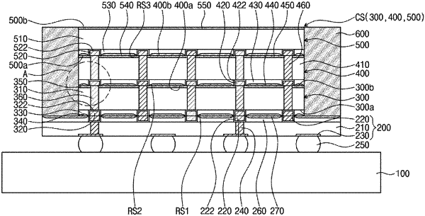
1. A method for manufacturing a semiconductor package, comprising:
mounting, on a substrate, a first semiconductor chip having a through electrode;
forming a second semiconductor chip;
disposing the second semiconductor chip on the first semiconductor chip such that a chip pad of the second semiconductor chip is in contact with the through electrode of the first semiconductor chip; and
forming a molding layer on the substrate,
wherein the forming of the second semiconductor chip includes:
forming a lower protective layer of a first insulation material on a bottom surface of a base layer having an integrated circuit;
forming the chip pad connected to the base layer through the lower protective layer;
etching a bottom surface of the lower protective layer to form a recess; and
filling an inside of the recess with a second insulation material to form an additional protective layer,
wherein a ductility of the second insulation material is greater than a ductility of the first insulation material, and
wherein, after disposing the second semiconductor chip on the first semiconductor chip, the through electrode and the chip pad are coupled to each other.
|