| CPC H01L 24/08 (2013.01) [H01L 21/76898 (2013.01); H01L 23/481 (2013.01); H01L 24/03 (2013.01); H01L 24/05 (2013.01); H01L 24/06 (2013.01); H01L 24/09 (2013.01); H01L 24/80 (2013.01); H01L 25/0657 (2013.01); H01L 25/50 (2013.01); H01L 24/94 (2013.01); H01L 2224/05147 (2013.01); H01L 2224/05181 (2013.01); H01L 2224/05184 (2013.01); H01L 2224/08146 (2013.01); H01L 2224/80896 (2013.01)] | 23 Claims |

|
1. A method of forming a microelectronic assembly, comprising:
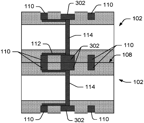
providing a first through substrate via (TSV) in a first substrate having a first surface;
forming a first metal contact pad in the first surface electrically coupled to and aligned over the first TSV;
forming a second metal contact pad in the first surface, the second metal contact pad having no TSV aligned thereunder, wherein the second metal contact pad has a smaller surface area at the first surface than the first metal contact pad; and
treating the first surface, the first metal contact pad and the second metal contact pad to form a first bonding surface for direct hybrid bonding.
|