| CPC H01L 23/552 (2013.01) [H01L 21/32051 (2013.01); H01L 21/561 (2013.01); H01L 21/78 (2013.01); H01L 23/3121 (2013.01); H01L 23/367 (2013.01); H01L 23/5383 (2013.01); H01L 24/16 (2013.01); H01L 24/81 (2013.01); H01L 24/97 (2013.01); H01L 25/16 (2013.01); H01L 27/0207 (2013.01); H01L 27/0617 (2013.01); H01L 2224/16227 (2013.01); H01L 2924/01022 (2013.01); H01L 2924/1431 (2013.01); H01L 2924/19041 (2013.01); H01L 2924/19105 (2013.01); H01L 2924/3025 (2013.01); H02M 1/08 (2013.01)] | 19 Claims |

|
1. A method of forming a power converter control circuit package, the method comprising:
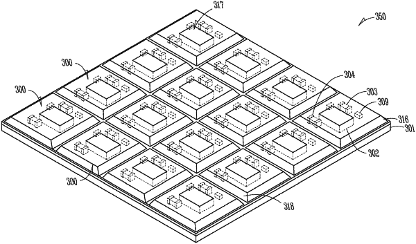
mounting an integrated circuit die and at least two passive devices on a substrate, the substrate supporting at least two conductive layers, and wherein a layout defined by locations of the at least two passive devices and electrical interconnections of the two passive devices provided by the substrate to the integrated circuit die are substantially symmetric about at least one axis;
covering an entirety of the at least two passive devices with an encapsulant to provide a panel of encapsulated power converter control packages;
defining an exposed region of the integrated circuit die with the encapsulant; and
electrically coupling at least a portion of the exposed region with a circuit defined by the integrated circuit die.
|