| CPC H01L 23/552 (2013.01) [H01L 23/66 (2013.01); H01L 24/17 (2013.01); H05K 1/0216 (2013.01); H05K 1/025 (2013.01); H01L 2223/6627 (2013.01)] | 17 Claims |

|
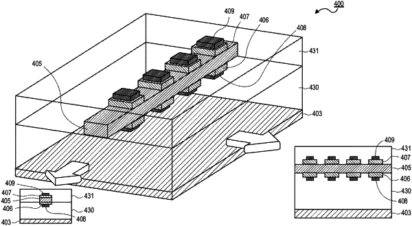
1. A package substrate, comprising:
a dielectric over a conductive layer;
a conductive line on the dielectric;
a plurality of conductive bumps on a surface of the conductive line, wherein the plurality of conductive bumps are conductively coupled to the conductive line and are embedded in the dielectric;
a plurality of metal features on the plurality of conductive bumps, wherein individual ones of the plurality of metal features are on a corresponding individual one of the plurality of conductive bumps, and wherein the plurality of metal features has a metal conductivity different than that of the plurality of conductive bumps; and
a solder resist over the conductive line and the dielectric.
|