| CPC H01L 23/535 (2013.01) [H01L 21/32136 (2013.01); H01L 21/76805 (2013.01); H01L 21/76819 (2013.01); H01L 21/76825 (2013.01); H01L 21/76895 (2013.01); H01L 23/5283 (2013.01); H01L 23/53257 (2013.01)] | 20 Claims |

|
1. A method of manufacturing a semiconductor device, comprising:
forming a first dielectric layer over a substrate;
forming a metal layer in the first dielectric layer;
forming an etch stop layer on a surface of the first dielectric layer and the metal layer;
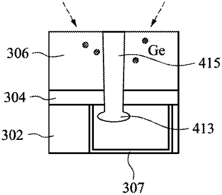
removing portions of the metal layer and the etch stop layer to form a recess in the metal layer, the recess being spaced apart from a bottom surface of the etch stop layer; and
forming a tungsten plug in the recess, wherein the metal layer includes cobalt, and first portions of the metal layer at or near a surface of the metal layer include an oxide of cobalt, and
wherein the method further comprises performing an etching operation using a fluoride containing gas to remove the first portions of the metal layer and remove second portions of the metal layer below the first portions to form the recess.
|
|
9. A method of manufacturing a semiconductor device, comprising:
forming a first dielectric layer over a substrate;
forming a cobalt plug in the first dielectric layer;
forming a nitride based etch stop layer on the first dielectric layer and the cobalt plug;
forming a second dielectric layer over the nitride based etch stop layer;
forming an opening in the second dielectric layer and the nitride based etch stop layer to expose an upper surface of the cobalt plug;
performing an etching operation using a fluoride containing gas to (1) remove one or more layers of an oxide of cobalt that is formed at or below the upper surface of the cobalt plug and (2) remove portions of the cobalt plug below the one or more layers of the oxide to extend the opening into the cobalt plug;
performing a defluorination process to remove the fluoride containing gas after the opening has been extended a desired distance into the cobalt plug;
forming a recess in the cobalt plug at a bottom of the opening, wherein the recess is spaced from the nitride based etch stop layer; and
forming a tungsten plug in the recess and the opening.
|
|
14. A method of manufacturing a semiconductor device, comprising:
forming a first dielectric layer over a substrate;
forming a cobalt plug in the first dielectric layer;
forming a nitride based etch stop layer on the first dielectric layer and the cobalt plug;
forming a second dielectric layer over the nitride based etch stop layer;
forming an opening in the second dielectric layer and the nitride based etch stop layer to expose an upper surface of the cobalt plug;
performing an etching operation using a fluoride containing gas to remove portions of the cobalt plug to extend the opening into the cobalt plug a desired distance from a bottom surface of the nitride based etch stop layer;
forming a recess in the cobalt plug at a bottom of the opening, wherein, in a cross-sectional view, the recess has a width that is at least greater than a width of a section of the opening located in the cobalt plug; and
forming a tungsten plug that is located in the recess, the opening, and on an upper surface of the second dielectric layer.
|