| CPC H01L 23/5283 (2013.01) [H01L 21/76816 (2013.01); H01L 21/76877 (2013.01); H01L 23/5226 (2013.01); H10B 41/27 (2023.02); H10B 41/41 (2023.02); H10B 43/27 (2023.02); H10B 43/40 (2023.02)] | 3 Claims |

|
1. A method for manufacturing a three-dimensional memory device, comprising:
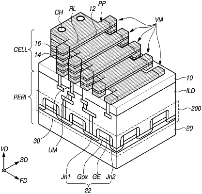
forming, on a substrate, a sacrificial layer including a plurality of sacrificial patterns for vias and a sacrificial pattern for a row line, which has a projection coupled to a corresponding sacrificial pattern for a via from among the plurality of sacrificial patterns for vias;
forming an interlayer dielectric layer that covers the sacrificial pattern for a row line and the sacrificial pattern for a via coupled to the sacrificial pattern for a row line and that has a plurality of holes exposing sacrificial patterns for vias, from among the plurality of sacrificial patterns for vias, that are not coupled to the sacrificial pattern for a row line;
forming a plurality of first conductive patterns in the plurality of holes;
repeating the forming of the sacrificial layer, the forming of the interlayer dielectric layer and the forming of the plurality of first conductive patterns to stack a plurality of sacrificial layers, a plurality of interlayer dielectric layers and a plurality of first conductive patterns on the substrate; and
replacing the plurality of sacrificial layers with a conductive material.
|