| CPC H01L 23/5283 (2013.01) [H01L 21/0228 (2013.01); H01L 21/30604 (2013.01); H01L 21/76831 (2013.01); H01L 21/76877 (2013.01); H01L 21/76898 (2013.01); H01L 23/481 (2013.01); H01L 23/5226 (2013.01)] | 20 Claims |

|
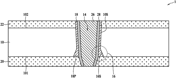
1. A semiconductor structure, comprising:
a substrate having a first surface and a second surface opposite to the first surface;
a conductive via through the substrate;
a first insulation layer between the substrate and the conductive via, wherein a first surface of the first insulation layer facing the substrate and a second surface of the first insulation layer facing the conductive via are extended along different directions;
a seed layer between the first insulation layer and the conductive via, wherein the first insulation layer is entirely separated from the conductive via by the seed layer; and
a second insulation layer over the second surface of the substrate, wherein a topmost surface of the first insulation layer, a top surface of the second insulation layer and a top surface of the conductive via are aligned with each other,
wherein the first insulation layer has a bottom surface aligned with the first surface of the substrate, and a width of the bottom surface of the first insulation layer is greater than a width of the topmost surface of the first insulation layer.
|