| CPC H01L 23/481 (2013.01) [H01L 21/76898 (2013.01); H01L 23/5286 (2013.01); H10B 10/12 (2023.02); H01L 23/50 (2013.01)] | 20 Claims |

|
1. An integrated circuit semiconductor device, comprising:
a substrate including a first surface and a second surface opposite the first surface;
a trench in the substrate, the trench extending from the first surface of the substrate toward the second surface of the substrate;
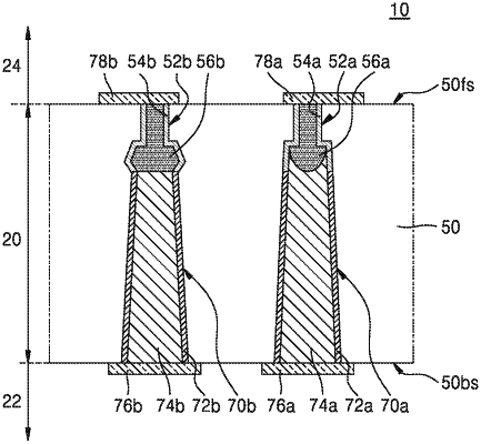
a through silicon via (TSV) landing part in the trench, the TSV landing part having:
a first portion spaced apart from the first surface of the substrate, and
a second portion between the first portion and the first surface of the substrate, the first portion being wider than the second portion;
a TSV hole in the substrate, the TSV hole extending from the second surface of the substrate and aligned with a bottom surface of the TSV landing part; and
a TSV in the TSV hole and in contact with the bottom surface of the TSV landing part wherein a width of the TSV increases and does not decrease in a direction from the first surface to the second surface.
|