| CPC H01L 23/46 (2013.01) [H01L 21/56 (2013.01); H01L 24/16 (2013.01); H01L 24/29 (2013.01); H01L 24/32 (2013.01); H01L 24/73 (2013.01); H01L 2224/16227 (2013.01); H01L 2224/29035 (2013.01); H01L 2224/32221 (2013.01); H01L 2224/73253 (2013.01)] | 17 Claims |

|
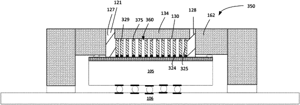
1. An integrated circuit (“IC”) package, comprising:
an IC die disposed on a printed circuit board (“PCB”), and
a temperature control element encasing the IC die, wherein the temperature control element comprises:
a plurality of thermal dissipating features disposed on a first surface of the IC die;
a manifold disposed on the PCB encasing the plurality of thermal dissipating features disposed on the IC die; and
a spacer disposed between the plurality of thermal dissipating features and the manifold,
wherein the plurality of thermal dissipating features comprises a metallic pin fin disposed on a solder bump.
|