| CPC H01L 23/373 (2013.01) [H01L 23/31 (2013.01); H01L 23/367 (2013.01); H01L 23/38 (2013.01); H01L 33/483 (2013.01); H01L 33/641 (2013.01); H01S 5/0231 (2021.01); H01S 5/02315 (2021.01)] | 7 Claims |

|
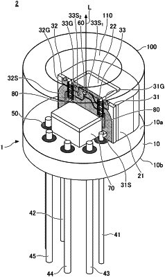
1. A header for a semiconductor package comprising:
an eyelet having an upper surface and a lower surface;
a first metal block molded integrally with the eyelet, protruding at the upper surface of the eyelet, and having a substantially U shape viewed from a normal direction of the upper surface of the eyelet;
a first lead sealed in a first through hole penetrating the eyelet from the upper surface to the lower surface of the eyelet;
a first substrate having a front surface formed with a first signal pattern electrically connected to the first lead and having a back surface that is an opposite side surface of the front surface, the back surface being fixed to a first end surface of the first metal block;
a second lead sealed in a second through hole penetrating the eyelet from the upper surface to the lower surface of the eyelet; and
a second substrate having a front surface formed with a second signal pattern electrically connected to the second lead and having a back surface that is an opposite side surface of the front surface of the second substrate, the back surface of the second substrate being fixed to a second end surface of the first metal block,
wherein a first portion that is a portion of the back surface of the first substrate and a second portion that is a portion of the back surface of the second substrate are exposed from the first metal block, and
wherein a ground pattern is formed on the first portion of the first substrate and a ground pattern is formed on the second portion of the second substrate.
|